search
Return

The chip automatic sorting equipment is one of HGTECH's automation products. It is a kind of highly efficient automated equipment with many functions, such as material connection platform, automatic scanning, robotic automatic lid removal, waste board edge and transplanting fixture suction, lid recycling, automatic QR code product identification by code readers, dual cross vacuum transplanting platform, automatic chip sorting, Jedec Tray automatic loading and unloading, dual cross tray material collecting transplanting, robotic transplanting carrier fixtures, automatic waste return, empty carrier ejection into box magazine, magazine automatic transplanting and return, vision positioning, image inspection and data processing.

The chip automatic sorting equipment is one of HGTECH's automation products. It is a kind of highly efficient automated equipment with many functions, such as material connection platform, automatic scanning, robotic automatic lid removal, waste board edge and transplanting fixture suction, lid recycling, automatic QR code product identification by code readers, dual cross vacuum transplanting platform, automatic chip sorting, Jedec Tray automatic loading and unloading, dual cross tray material collecting transplanting, robotic transplanting carrier fixtures, automatic waste return, empty carrier ejection into box magazine, magazine automatic transplanting and return, vision positioning, image inspection and data processing.


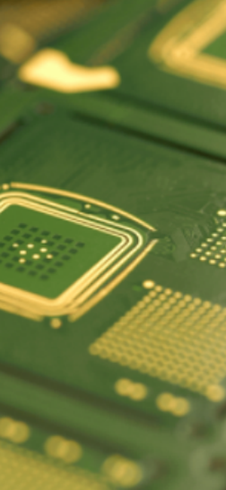
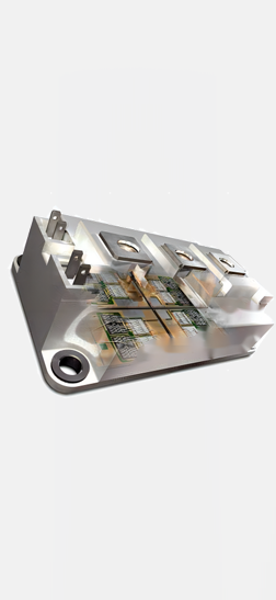
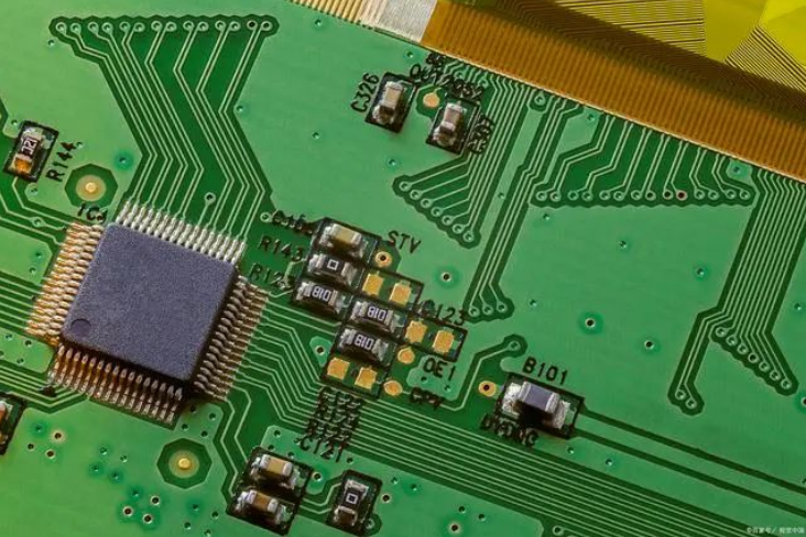
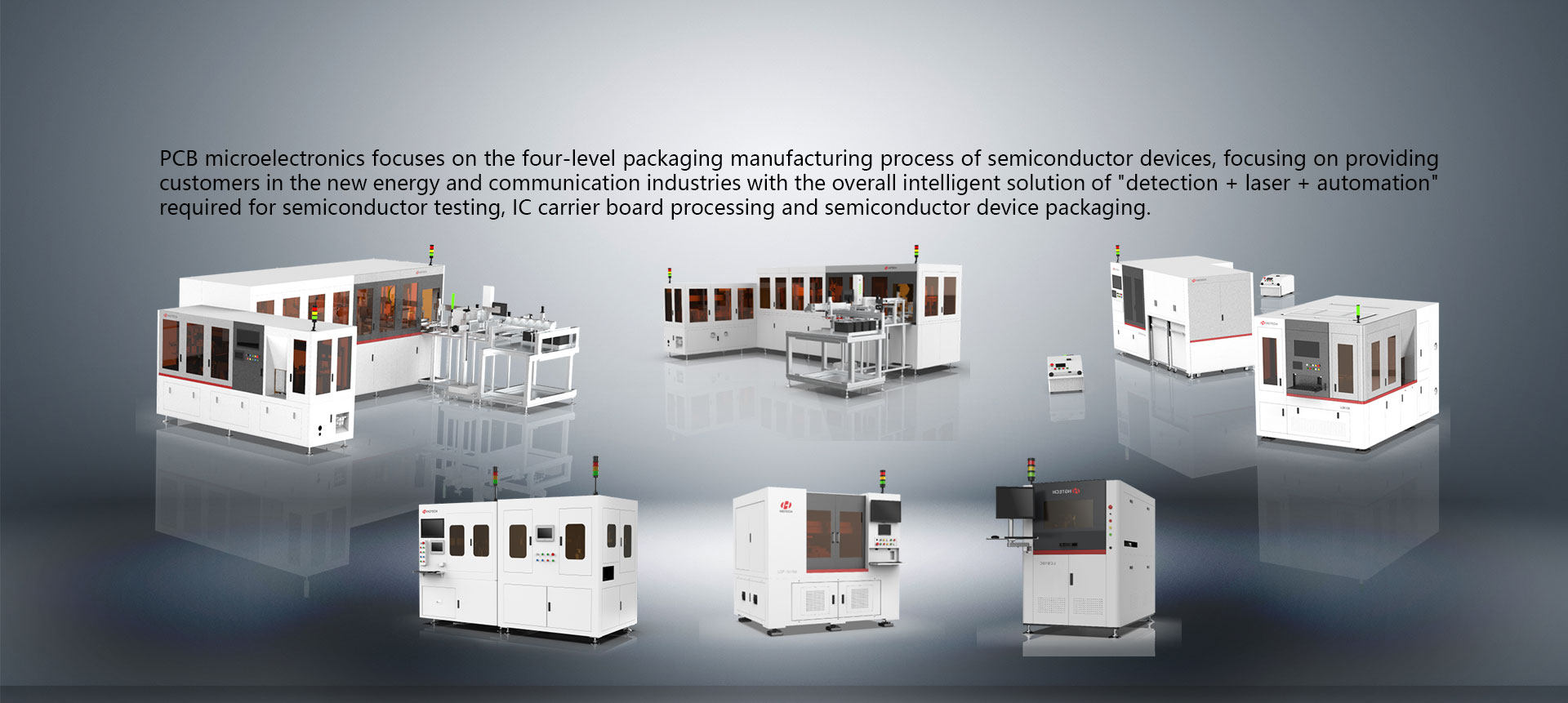
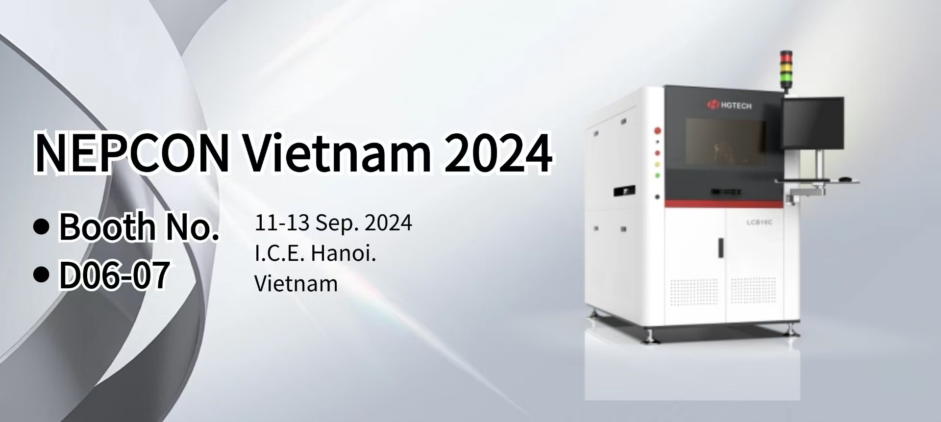
The PCB Microelectronics Division was established in 2016, with a research and development center, a process center, and three product lines. It is a leading enterprise in China's IC carrier intelligent equipment, and relies on the visual laboratory platform of the Central Research Institute of Huagong Technology to build a leading domestic semiconductor testing equipment enterprise. PCB microelectronics revolves around the two fundamental materials of the microelectronic component industry chain - carrier board+chip, and extends to the upstream substrate/wafer of the industry chain and downstream chip packaging and device assembly fields for layout, providing a full process intelligent solution of "laser+packaging+detection".
INNOVATION FUELS A BETTER WORLD